
loading...
VLSI Design Course with Certification
The Industry and Govt.of Karnataka acknowledges the pressing need to address the increasing demand for skilled professionals in the field of VLSI (Very Large Scale Integration) Design. With rapid technological advancements, VLSI plays a crucial role in sectors such as telecommunications, automotive, healthcare, and consumer electronics. However, there is a significant shortage of trained individuals possessing the necessary knowledge and expertise in VLSI Design.
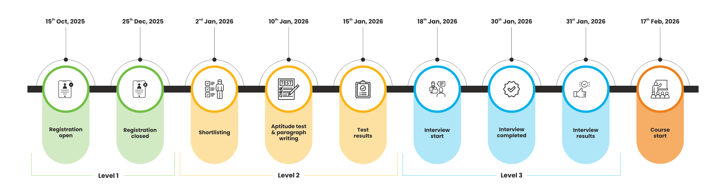
To tackle this critical requirement, we are delighted to launch the Next Generation K-VLSI Design Program, in collaboration with the MINRO Center at IIIT Bangalore, IESA, and SAFL. This intensive 6-9 month skill development pilot program is specifically tailored for VLSI Design, aiming to equip students with the essential skills and make them job-ready for the thriving ESDM industry.


Engineers from Electronics, ECE, CS, IT and related engineering branches


Program Fee: The overall value of the program is ₹ 2,50,000 + GST. However, the shortlisted candidate will only pay Rs. 15,000


NOTE:- Decision taken by Futurewiz Management in regard to test/interview/selection - will be final
1SOC Architecture Introduction
2Digital
3Analog Design Introduction
4Design Flow
5Design Architecture, RISC-V & ARM
6 Verification - Introduction
7Introduction to Emulation
8 DFT Basics (Scan, JTAG, BIST)
9Introduction to Synthesis & Timing Constraints
10Placement, Routing & CTS
11Validation
12 C and OOPs Basics
13Verilog & System Verilog
14Embedded Software
15Python Scripting
16Mini Projects (frontend & backend)
17 Major Project (frontend/backend)
18Summary
We really appreciate you taking the time to get in touch. Please fill in the form for any further queries.

