loading...



The answer is chip design isn't one job; it's a relay race with 10 stages, each handled by specialized engineers. Understanding this flow isn't just interesting trivia; it's the roadmap for figuring out where you want to specialize, whether that's RTL design, verification, or physical design (PD).
Let's walk through the entire journey, step by step.
1. Architecture
Every chip starts as a requirement or specification, not a line of code. Architects define the use case and features. Is this chip for a smartphone, a data center, or an IoT sensor? They also lock down the PPA targets- Performance, Power, and Area. Every decision made downstream traces back to choices made here. Get the architecture wrong, and no amount of clever coding later can fix it.
2. RTL Design
This is where the architecture turns into actual hardware description code, written in Verilog or SystemVerilog. RTL (Register Transfer Level) designers translate the micro-architecture the detailed internal logic, pipelines, and data paths into synthesizable code If you enjoy digital logic, hardware architecture, coding, and thinking in terms of clocks, registers, data paths, and state machines, This is a natural entry point into the industry.
3. Functional Verification
Here's a stat that surprises most students: verification engineers often outnumber design engineers on a project. Why? Because a single bug that slips through to silicon can cost millions of dollars and months of delay. Verification engineers build testbenches, often using UVM (Universal Verification Methodology), to simulate the RTL design against thousands of scenarios and measure functional coverage to ensure every corner case has been exercised. If you like breaking things systematically and thinking like a detective, verification is an excellent career path and it's also one of the fastest-growing and highest-paying specializations in VLSI today.
4. Synthesis
Once RTL is verified, it needs to become something that can actually be built in silicon. Synthesis tools convert your RTL into a gate-level netlist a collection of standard logic gates (AND, OR, flip-flops, etc.) connected together. This stage also involves the first real trade-offs between timing, area, and power, guided by constraints the design team provides.
5. DFT (Design for Testability)
Here's something students rarely think about: how do you test a finished chip after it's manufactured, when you can't exactly attach a debugger to it? That's what DFT solves. Engineers insert structures like scan chains, MBIST (Memory Built-In Self-Test), and JTAG interfaces into the design, so that every manufactured chip can be tested for defects on the production line, quickly and reliably.
DFT is therefore an essential bridge between chip design and manufacturing test.
6. Physical Design (PD)
This is where the netlist becomes an actual physical layout. PD engineers handle floor-planning (deciding where major blocks sit on the die), placement of individual cells, Clock Tree Synthesis (CTS) to distribute the clock signal evenly across the chip, and routing to physically connect everything with metal wires. It's a highly visual, puzzle-like discipline a favorite for students who enjoy optimization problems.
7. STA (Static Timing Analysis)
Before the design can be released for manufacturing, it must pass several sign-off checks.. STA checks timing across all corners different combinations of voltage, temperature, and process variation to make sure no signal arrives too late or too early. This is the sign-off stage: nothing moves forward until STA gives the green light.
8. Tape-Out
Tape-out is the moment of truth. The final design is converted into GDSII format essentially the master blueprint of the chip and formally signed off and sent to the foundry for manufacturing. It's called “tape-out” as a nod to the days when this data was literally sent out on magnetic tape. Once a design tapes out, there's no going back without enormous cost, so every prior stage exists to make this moment as safe as possible.
9. Fabrication
Now the chip leaves the digital world and enters a cleanroom. Wafer processing at the foundry (think TSMC, Samsung, or GlobalFoundries) etches billions of transistors onto a silicon wafer using photolithography, layer by layer. Once wafers are diced into individual dies, each chip goes through packaging, where it's encased and connected to the pins or balls that let it interface with a circuit board.
10. Silicon Validation & Bring-Up
Finally, the very first real chips come back from the fab, and engineers perform board bring-up powering on the chip for the first time on a test board and checking that it behaves as designed. This stage, validation on silicon, is where all the simulation and analysis from earlier stages gets confirmed (or occasionally, humbling surprises show up that require a re-spin).
Why This Matters for Your Career
Notice something important: this flow isn't a single job description it's an entire industry's worth of specialized roles. As a final-year engineering student preparing to enter the semiconductor industry, understanding the complete chip development flow can help you identify the area that best matches your interests and skills.
Interested in manufacturing tests and improving test coverage? → DFT
Enjoy timing analysis and mathematical problem-solving? → STA / Timing Analysis
Enjoy timing analysis and mathematical problem-solving? → STA / Timing Analysis
At FutureWiz, our training programmes are built around exactly this flow: we teach RTL design, functional verification with UVM, and physical design as complete, industry-aligned tracks, so you graduate not just knowing the theory but ready to contribute to a real tape-out from day one.
Understanding “how a chip is built” is step one. The next step is deciding which part of this flow you want to master. Explore our courses to find yours.
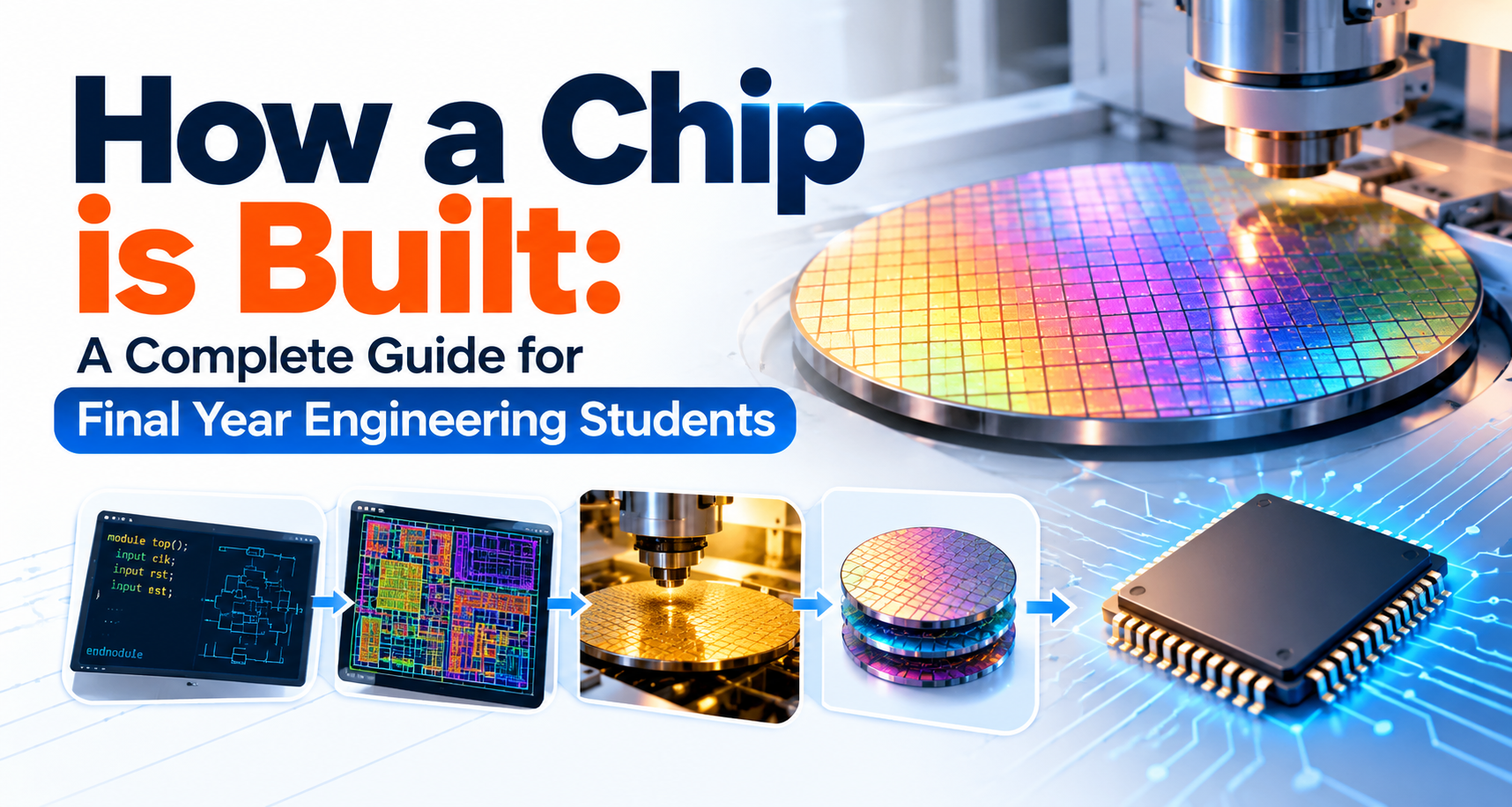 How a Chip is Built: A Complete Guide for Final Year Engineering Students
 Verilog vs SystemVerilog - A Complete Guide for VLSI Learners
 How to Build a Killer VLSI Portfolio in College (5 Projects Every Student Should Do)
 RTL Design Best Practices That 90% of Freshers Ignore (But Companies Love)
 Digital VLSI vs Analog VLSI vs Mixed-Signal – Which One Should You Choose in 2026?
 Designing VLSI Circuits for Quantum Machine Learning Algorithms
 Online vs. Traditional VLSI Physical Design Courses: Pros and Cons
 Advances in VLSI Design for Artificial Intelligence Applications
 Choosing the Right VLSI Training Institute: Factors to Consider
 VLSI Design for Energy-Efficient Wireless Sensor Networks
 How to Become a VLSI Chip Designer: A Beginner's Roadmap for 2026
 A to Z on India, Japan & the Future of Semiconductor Industry: A New Chapter in Tech Collaboration
 RTL Design vs Physical Design: What's the Real Difference?
 The Future of the Semiconductor Industry: What Indian Students Should Know
 Top 7 Career Paths After Completing a VLSI Course
 Best Time Management Tips for Students Preparing for VLSI Careers
 Mastering VLSI Physical Design: A Comprehensive Course Overview
 The Complete FPGA and ASIC Guide
 Verilog Essentials: Mastering the Fundamentals of Hardware Description Language
 Unleashing the Power of System Verilog: A Comprehensive Guide for Aspiring Designers
 Demystifying VLSI chip Design: Exploring the Core Concepts of VLSI Courses
 Basics of VLSI - An Ultimate Guide
 Career Prospects After Completing A VLSI Course
 Top 5 Reasons To Take Up A Professional VLSI Course
 Mastering VLSI Design: A Comprehensive Guide To Understanding Complex Integrated Circuits
 Future-Proof Your Career With A VLSI Course: How Learning About Integrated Circuits Can Boost Your Job Prospects?
 System Verilog: An Overview
 Introduction to Hardware Description Language (HDL)
 Unlock The Potential Of VLSI Design With An Integrated VLSI Course Online
 Universal Verification Methodology:An Efficient Verification Approach
 How to Write a Verilog Module for Design and Testbench
 What Are the Different Career Paths in the VLSI Industry?