loading...
The first integrated circuits contained a few transistors and were called SSI (Small scale integration). They incorporated circuits having transistors numbering to tens. They were followed by devices that held hundreds of transistor in a chip and were called MSI (Medium scale integration). These were followed by introduction of LSI (Large scale integration) and VLSI (Very large scale integration).
VLSI is the process of creating an Integrated circuit (IC) by combining thousands of resistors in a chip. VLSI started in 1970s when complex semiconductor technologies were being defined. Before VLSI most ICs had limited set of functions to perform. Over the last few decades there has been rapid development in large scale integrated circuits.
Following diagram shows the Design flow from Specification to Post-Si Validation.
All the above stages from Specification to Functional Verification are called Front end and stages from logic synthesis to fabrication are called back end.
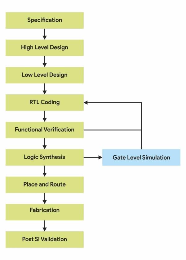
Figure 1: Design Flow
Specification: Defines the functionality, interface, architecture of the IC
Behavioural description defines the functionality, performance and compliance to standard for the design.
Hardware Design Language is used to define the RTL. RTL is simulated to test the functionality. Simulators are needed at this stage. RTL is then converted to gate level netlist using logic synthesis tools. A gate level netlist describes the design in terms of gates and connections.
After this a physical layout is made and verified before sending for fabrication.
High Level Design: The design architecture is defined at this stage. Various functional blocks and the interface communication protocols are defined at this stage.
Low Level Design: In this phase the microarchitecture is defined. It involves the modules, state machines, counters, registers etc.
RTL Coding: Hardware Design language (HDL) is used for developing synthesizable constructs.
Functional Verification: Functional characteristics of design, correct behaviour of design is verified in this stage.
Logic Synthesis: Some design compiler takes the RTL and maps it to target technology.
Placement and Routing: All the gates and flip flops are placed, Clock tree synthesis is done and reset is routed. GDS file output happens after each block is routed. This is used in foundry for fabricating ASIC.
Gate level Simulation: Timing information of gates is created by the placement and routing tool. Here the output is in form of a SDF (standard delay file). A static timing analysis tool can also be used to perform static timing analysis checks.
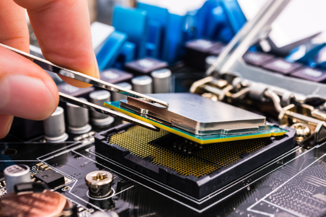
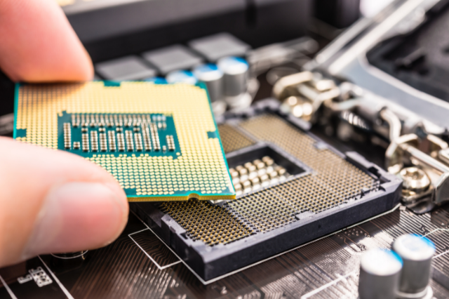
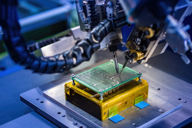
Fabrication: The final GDS file is sent to foundry which fabricates silicon. After fabrication, packaging is done and chip is ready for testing.
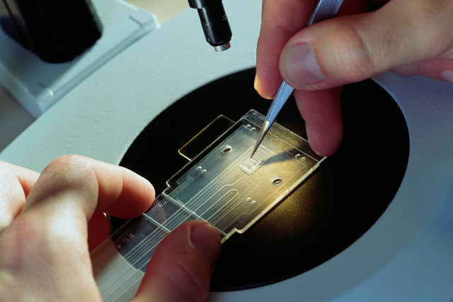
Post silicon validation: Before chip can be widely marketed, it is put into a test environment where it can be tested. This test is done in labs using firmware that programs the chip.
Benefits of VLSI
Cost effective
Low power
Improved speeds
Takes less space
Enhanced reliability
Career opportunities for Front end and back end engineers
On the front end an engineer can start as a RTL design engineer or verification engineer and gain knowledge and skills as they advance in their career. A diversion to architecture development can be done by system architects.
On the back end, engineers can do placement, routing, timing analysis. Both front end and back end engineers have enough opportunities available.
Verification, Validation, Testing of ASIC
Verification is a common term used in ASIC design cycle. Verification is a process where the design is tested against a design specification before tape-out. The main purpose here is to check the design correctness before tapeout. Design simulation is a popular method for verification but it has also expanded to do power simulation, formal property verification and static and dynamic checks.
In Validation the manufactured chip is tested for correctness in a lab. This is done in a test board or reference board. Validation starts with individual features of chip, but involves other stress testing of all features. It involves both software and hardware. Validation is also done based on chip availability therefore pre-silicon and post -silicon validation is done.
Testing involves manufactured chips for defects. First level testing at wafer level, that involves various technology and transistor parameters before the die is available. Next level testing happens on a packaged die. Next level testing involved digging out manufacturing faults. After this characterization of chip is done, involving voltage frequency level testing to generate ideal operating conditions.
To obtain optimum coverage and run, functional test patterns are used and functional defects are identified.
Future of VLSI
VLSI has been succeeded by ULSI (Ultra large scale integration). It was designed to get highest computational power from smallest microchip. This incorporated microchip with more than million transistors. Intel Pentium and 486 series were built using ULSI principles.
 Verilog Essentials: Mastering the Fundamentals of Hardware Description Language
 Unleashing the Power of System Verilog: A Comprehensive Guide for Aspiring Designers
 Demystifying VLSI ch Design: Exploring the Core Concepts of VLSI Courses
 Basics of VLSI - An Ultimate Guide
 Career Prospects After Completing A VLSI Course
 Top 5 Reasons To Take Up A Professional VLSI Course
 Mastering VLSI Design: A Comprehensive Guide To Understanding Complex Integrated Circuits
 Future-Proof Your Career With A VLSI Course: How Learning About Integrated Circuits Can Boost Your Job Prospects?
 System Verilog: An Overview
 Introduction to Hardware Description Language (HDL)
 Unlock The Potential Of VLSI Design With An Integrated VLSI Course Online
 Universal Verification Methodology:An Efficient Verification Approach
 How to Write a Verilog Module for Design and Testbench
 What Are the Different Career Paths in the VLSI Industry?
 Skills required to establish a successful career in VLSI
 Looking for online VLSI courses? Futurewiz can fulfill your upskilling needs!
 The Future Of VLSI- Get All The Latest Insights!
 Super 50 Program For Advanced VLSI Design TrainingSteps to Build Career in VLSI
 Similarities between C and Verilog
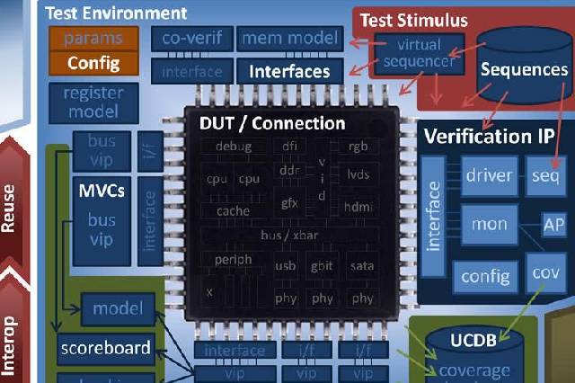 What is UVM - A High-level overview