loading...
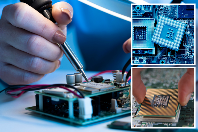
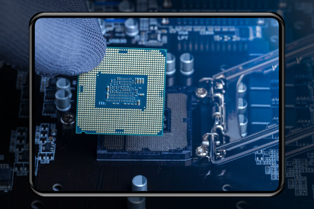
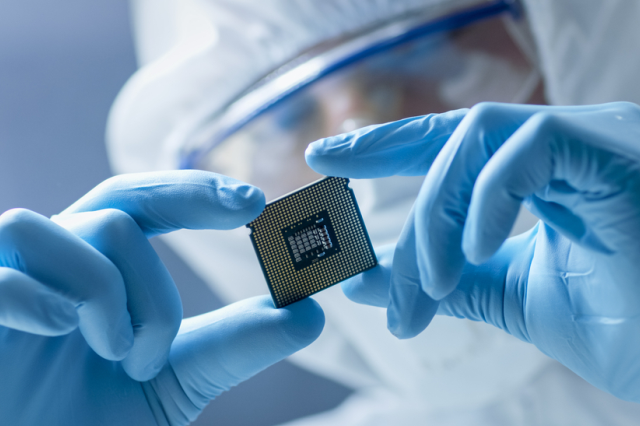
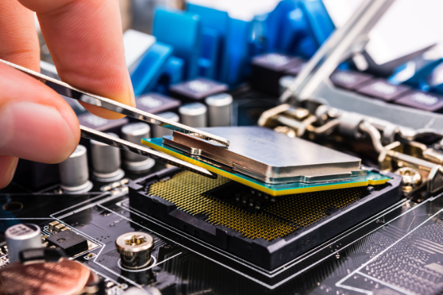
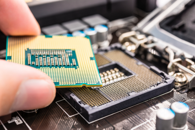
Very Large Scale Integration (VLSI) Design is a critical part of the modern electronics industry. VLSI refers to the process of creating an integrated circuit (IC) with millions or even billions of transistors on a single chip. VLSI has revolutionized the electronics industry by allowing for the creation of smaller, faster, and more powerful electronic devices.
Mastering the VLSI design course requires a comprehensive understanding of complex integrated circuits, as well as the processes involved in designing and manufacturing these circuits.
This article will provide an overview of VLSI Design and highlight some key aspects of the design process.
Overview of VLSI Design
The VLSI design process involves several stages, including:
Specification
In this stage, the requirements and specifications for the IC are defined. This includes identifying the intended use of the IC, as well as any performance requirements or constraints.
Architecture
The architecture stage involves determining the overall structure and functionality of the IC. This includes deciding on the number and type of components that will be included on the chip, as well as how they will be interconnected.
Logic Design
The logic design stage involves creating a digital circuit diagram that specifies the behavior of the IC. This diagram is used to generate a hardware description language (HDL) code that can be used to program the IC.
Verification
The verification stage involves testing the logic design to ensure that it meets the specifications and requirements of the IC.
Physical Design
The physical design stage involves creating a layout of the IC that specifies the location and arrangement of components on the chip.
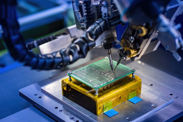
Fabrication
The fabrication stage involves manufacturing the IC using various processes, including lithography, deposition, etching, and doping.
Testing
The testing stage involves verifying that the IC functions as intended and meets the performance requirements.
Key Aspects of VLSI Design
Transistor Sizing
One of the key challenges in VLSI design is determining the optimal size for each transistor on the chip. Transistor sizing involves balancing performance and power consumption, as smaller transistors generally offer better performance but consume more power.
Power Optimization
Power optimization is another critical aspect of VLSI design, as the power consumed by the IC can have a significant impact on its performance and lifespan. Power optimization techniques include clock gating, voltage scaling, and power gating.
Physical Design Challenges
The physical design of the IC can also present significant challenges, including routing, placement, and floorplanning. These challenges become more pronounced as the number of components on the chip increases.
Design for Testability
Design for testability (DFT) refers to designing the IC in a way that makes it easier to test and diagnose any faults or errors. DFT techniques include scan chains, boundary scan, and built-in self-test (BIST).
Design for Manufacturability
Design for manufacturability (DFM) is designing the IC in a way that makes it easier and more cost-effective to manufacture. DFM techniques include reducing the number of process steps, optimizing process parameters, and designing the IC to be more resilient to manufacturing variations.
VLSI Design is a complex and challenging field that requires a comprehensive understanding of integrated circuits and the design and manufacturing processes involved. By mastering the VLSI training, designers can create high-performance, low-power ICs that meet the demanding requirements of modern electronic devices.
Choosing FutureWiz For Best VLSI Training In Noida
Choosing FutureWiz for online VLSI courses is an excellent decision for those seeking to enhance their skills and secure employability in the Semiconductor/VLSI/EDA industry. With a focus on skill development and an emphasis on practical, industry-relevant training, our dynamic VLSI courses are structured and presented by industry specialists.
We offer a predominant training methodology and infrastructure that provides students with the opportunity to gain hands-on experience and develop the necessary expertise to excel in their careers. Additionally, we provide 100% placement assistance to our students, ensuring they secure confirmed jobs in the industry. At FutureWiz, we are committed to empowering the next generation of skilled millennials and preparing them for a successful future in the VLSI industry.
 Verilog Essentials: Mastering the Fundamentals of Hardware Description Language
 Unleashing the Power of System Verilog: A Comprehensive Guide for Aspiring Designers
 Demystifying VLSI ch Design: Exploring the Core Concepts of VLSI Courses
 Basics of VLSI - An Ultimate Guide
 Career Prospects After Completing A VLSI Course
 Top 5 Reasons To Take Up A Professional VLSI Course
 Mastering VLSI Design: A Comprehensive Guide To Understanding Complex Integrated Circuits
 Future-Proof Your Career With A VLSI Course: How Learning About Integrated Circuits Can Boost Your Job Prospects?
 System Verilog: An Overview
 Introduction to Hardware Description Language (HDL)
 Unlock The Potential Of VLSI Design With An Integrated VLSI Course Online
 Universal Verification Methodology:An Efficient Verification Approach
 How to Write a Verilog Module for Design and Testbench
 What Are the Different Career Paths in the VLSI Industry?
 Skills required to establish a successful career in VLSI
 Looking for online VLSI courses? Futurewiz can fulfill your upskilling needs!
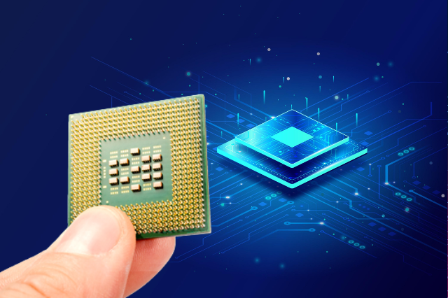 The Future Of VLSI- Get All The Latest Insights!
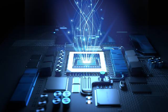 Super 50 Program For Advanced VLSI Design TrainingSteps to Build Career in VLSI
 Similarities between C and Verilog
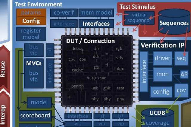 What is UVM - A High-level overview