loading...
This article will give the way Module keywords are used to structure Verilog designs and how this relates to the hardware being described. The main purpose of this post is to introduce the skills which will allow us to model and test our digital design.Our discussion will start with the basic components of Verilog code.
A Verilog module is an essential building block that defines a design or testbench component by specifying the block's ports and internal behaviors. A module provides the necessary functionality to the higher-level block through its port interface. Module declaration comes on top of every Verilog program.To develop hierarchical architectures, higher-level modules can embed lower-level modules.
Verilog ports are the medium to connect Verilog modules with one another to communicate. Verilog is structured simply. Apart from system tasks and functions which are made global, all data, functions, and tasks are written in modules.
A Verilog module is enclosed between the keywords module and endmodule. The Verilog module has several components such as:
Lets understand each component one by one.
Module:Module is declared by the keyword module.A corresponding keyword endmodule must appear at the end of the module definition.Each module must have a module name, which is the identifierfor the module, and a port list, which describes the input and output terminals of the module.
Ports: are the pins or signal which act as input or output of a specified module.Port list is an important component of Verilog module which provide a means for a module to communicate with the external world through input and output.There are three types of port available in Verilog:
All ports declared as one of the above are assumed to be awire by default, otherwise it is necessary to declare it again. Declaring multiple ports with same name is illegal. Module declaration syntax is shown below:
|
modulemodule_name (portdefinition); // Body of Module endmodule |
|
modulemodule_name ; //port list can be empty for testbench // Body of Module endmodule |
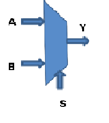
So, module for given logical circuit can written as:
|
module mux1(input A, B, S, outputY) ; // Body of Module endmodule |
Parameter:is defining a constant which can be set when you use a module, which allows customization of module during the instantiation process.It can be a binary , Integer, real or string.
Syntax:parameter variable_name = value;
Module body: In essence, the "code that is inside the module" (following the port declaration) is referred to as a module body. It specifies what makes up the module and may contain a wide variety of declarations and definitions (such as net and variable declarations, always blocks and initial blocks, etc.).In Verilog, a module body can be defined using various levels of abstraction. There are four levels of abstraction in Verilog: -
Gate Level
Within the logical level, the characteristics of a system are described by logical links and their timing properties. All signals are discrete signals. They can only have definite logical values (`0', `1', `X', `Z`). The usable operations are predefined logic primitives (basic gates). Gate level modelling may not be a right idea for logic design. Gate level code is generated using tools like synthesis tools and this netlist is used for gate level simulation and for backend.
Register−Transfer Level
Designs using the Register−Transfer Level specify the characteristics of a circuit using operations and the transfer of data between the registers. The modern definition of an RTL code is "Any code that is synthesizable is called RTL code".
Behavioral level
This level describes a system by concurrent algorithms (Behavioural). Every algorithm is sequential, which means it consists of a set of instructions that are executed one by one. Functions, tasks, and procedural blocks are the main elements. There is no regard to the structural realization of the design.
This section will give you the flavor of Verilog coding for design with different levels of abstraction. For example, a 2:1 multiplexer as discussed above is taken to explain to you the different styles of coding using Verilog.
|
module mux1(input A, B, S, outputY) ; // using Gate level modeling // Y= S’.A+ S.B wire w1,w2,w3; not (w1,S); // w1=S’ and (w2, w1,A); //w2= S’.A and (w3,S, B); //w3= S.B or (Y, w2,w3); //Y= S’.A+S.B endmodule |
|
module mux1(input A, B, S, outputY) ; // Using RTL Coding assign Y= S? B: A; endmodule |
|
module mux1(input A, B, S, outputregY); // Using Behavioral Code always @(*) begin if(S) Y= B; else Y=A; end endmodule |
Now we understand the approach to writing a testbench for the Design / top-level module, which we have learned in the above section. This section will discuss the basic architecture of Verilog testbench. When a digital design is being implemented using Verilog, we normally also create a testbench to stimulate the code and ensure that it functions as expected.The testbench can be written in several languages, the most popular being VHDL, Verilog, and System Verilog.Testbenches contain non-synthesizable Verilog code that generates inputs for the design and verifies that the outputs are accurate. A Verilog testbench is consisting of:
|
module mux1_tb; reg A,B,S; wire Y; // Testbench Code endmodule |
|
//DUT Instantiation with positional Port mux1 DUT (A,B,S,Y); |
|
//DUT Instantiation with named Port mux1 DUT (.A(A),.B(B),.S(S),.Y(Y)); |
|
// Generate Clock initial begin clk= 1’b0; forever #2 clk= ~clk; end |
|
// Generatethe Reset initial begin reset= 1’b1; #8 reset= 1’b0; end |
Writing the stimulus: The next part of the testbench is stimulus generation. We must generate each of the possible input combinations to test the circuit. After every combination, we then need to wait for a short time while the signals propagate through our code block. To do this, we assign the values to inputs and then use the Verilog delay operator. The below code snippet illustrates the code for this.
|
// Generate the input combination after 2 unit delay initial begin A= 1’b0; B= 1’b0; S= 1’b0; #2 A= 1’b0; B= 1’b0; S= 1’b1; #2 A= 1’b0; B= 1’b1; S= 1’b0; #2 A= 1’b0; B= 1’b1; S= 1’b1; #2 A= 1’b1; B= 1’b0; S= 1’b0; #2 A= 1’b1; B= 1’b0; S= 1’b1; #2 A= 1’b1; B= 1’b1; S= 1’b0; #2 A= 1’b1; B= 1’b1; S= 1’b1; end |
|
// Monitor the inputs and outputs initial begin $monitor (“ Sim Time=%t, A=%b, B=%b, S=%b, Y=%b”, $time, A, B, S, Y); end |
Complete Verilog code for Design and Testbench: By combining all parts of Testbench, full Verilog code for 2:1 MUX Design and Testbench is shown below.
|
// Testbench Code for 2:1 MUX DUT module mux1_tb; reg A,B,S; wire Y; //DUT Instantiation mux1 DUT (.A(A),.B(B),.S(S),.Y(Y)); // Generate the input combination after 2 unit delay initial begin A= 1’b0; B= 1’b0; S= 1’b0; #2 A= 1’b0; B= 1’b0; S= 1’b1; #2 A= 1’b0; B= 1’b1; S= 1’b0; #2 A= 1’b0; B= 1’b1; S= 1’b1; #2 A= 1’b1; B= 1’b0; S= 1’b0; #2 A= 1’b1; B= 1’b0; S= 1’b1; #2 A= 1’b1; B= 1’b1; S= 1’b0; #2 A= 1’b1; B= 1’b1; S= 1’b1; end // Monitor the inputs and outputs initial begin $monitor (“ Sim Time=%t, A=%b, B=%b, S=%b, Y=%b”, $time, A, B, S, Y); end endmodule |
|
// Verilog code for 2:1 MUX module mux1(input A, B, S, outputY); // Using RTL Coding Ternary operator assign Y= S? B: A; endmodule |
|
// Verilog code for 2:1 MUX module mux1(input A, B, S, outputY); // Using RTL Coding using Data flow assign Y= (~S & A) | (S & B); endmodule |
|
// Verilog code for 2:1 MUX module mux1(input A, B, S, outputregY); // Using Behavioral Code always @(*) begin if(S) Y= B; else Y=A; end endmodule |
 Verilog Essentials: Mastering the Fundamentals of Hardware Description Language
 Unleashing the Power of System Verilog: A Comprehensive Guide for Aspiring Designers
 Demystifying VLSI ch Design: Exploring the Core Concepts of VLSI Courses
 Basics of VLSI - An Ultimate Guide
 Career Prospects After Completing A VLSI Course
 Top 5 Reasons To Take Up A Professional VLSI Course
 Mastering VLSI Design: A Comprehensive Guide To Understanding Complex Integrated Circuits
 Future-Proof Your Career With A VLSI Course: How Learning About Integrated Circuits Can Boost Your Job Prospects?
 System Verilog: An Overview
 Introduction to Hardware Description Language (HDL)
 Unlock The Potential Of VLSI Design With An Integrated VLSI Course Online
 Universal Verification Methodology:An Efficient Verification Approach
 How to Write a Verilog Module for Design and Testbench
 What Are the Different Career Paths in the VLSI Industry?
 Skills required to establish a successful career in VLSI
 Looking for online VLSI courses? Futurewiz can fulfill your upskilling needs!
 The Future Of VLSI- Get All The Latest Insights!
 Super 50 Program For Advanced VLSI Design TrainingSteps to Build Career in VLSI
 Similarities between C and Verilog
 What is UVM - A High-level overview